Large-Area 3D Optical Surface Profilometer
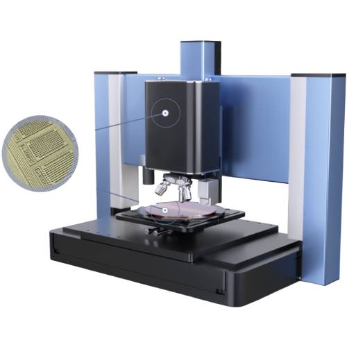


Large-Area 3D Optical Surface Profilometer is a high-performance three-dimensional optical metrology system designed for large-area surface topography measurement. It combines high-speed scanning, multiple imaging technologies, and ultra-high vertical resolution to deliver accurate and repeatable 3D surface data across a wide range of sample sizes and material types. By integrating six imaging and analysis methods on a single platform, this system enables nanoscale surface characterization while maintaining excellent efficiency and measurement flexibility.
Application
The Large-Area 3D Optical Surface Profilometer is suitable for surface morphology analysis and dimensional evaluation of various materials and components, including but not limited to:
Semiconductor wafers and microelectronic devices
Thin films and optical coatings
Precision mechanical components
Functional surfaces with large slopes or low reflectivity
Transparent or multilayer materials
Micro- and nano-structured surfaces
Typical test objects include wafers, devices, thin films, coated components, and precision assemblies requiring large-area, high-resolution surface measurement.
Standards
The system’s analysis capabilities and software design support surface metrology requirements defined in relevant international standards, including but not limited to:
ISO 25178 (Surface texture: Areal)
ISO 4287 / ISO 4288 (Surface roughness parameters and evaluation)
ISO 16610 (Filtration of surface texture)
ISO standards for optical surface measurement and reporting
Parameters
| Parameter | Specification |
|---|---|
| Imaging speed | High-speed camera up to 200 FPS |
| Z-axis resolution | Sub-nanometer resolution, independent of objective magnification or scan range |
| Imaging technologies | White light interferometry, confocal, spectral film thickness, bright field, dark field, zoom imaging, AFM |
| XY stage | Modular precision XY stage, customizable up to 300 × 300 mm |
| Sample compatibility | Wafers, devices, thin films, components, large-area samples |
| Software | ISO-compliant analysis software with automated measurement and reporting |
Features
Six-in-one integrated imaging and analysis platform
High-speed camera enabling rapid surface acquisition
Sub-nanometer vertical resolution for precise height measurement
Modular and scalable platform for large-area samples
High-resolution spinning disk confocal scanning for fast area imaging
Physical suppression of scattered light to improve image contrast and accuracy
Advanced software for automated analysis and standardized report generation
Accessories
Precision modular XY stage (up to 300 × 300 mm)
High-speed imaging camera
Confocal scanning module
White light interferometry module
Thin film thickness measurement module
AFM measurement module
Maintenance Information
Keep optical components clean to maintain measurement accuracy and image quality.
Periodically inspect the XY stage and motion system for smooth operation.
Ensure the system operates within the specified environmental conditions.
Perform routine software updates and calibration as recommended to maintain compliance with measurement standards.
FAQ
1. What makes the Large-Area 3D Optical Surface Profilometer suitable for large samples?
The system is built on a modular platform that supports a precision XY stage customizable up to 300 × 300 mm. This allows stable and accurate measurement of large-area samples such as wafers, devices, and assembled components. High-speed scanning and automated analysis further ensure that expanding the measurement area does not compromise efficiency or data consistency.
2. How does the six-in-one imaging configuration improve measurement capability?
By integrating white light interferometry, confocal imaging, spectral film thickness measurement, bright field, dark field, zoom imaging, and AFM on a single platform, the system can handle a wide range of surface types. Smooth, rough, transparent, low-reflectivity, and multilayer samples can all be measured with appropriate techniques, enabling nanoscale resolution and comprehensive surface characterization without changing instruments.
3. Why is spinning disk confocal scanning faster than traditional confocal methods?
Spinning disk confocal scanning uses multiple pinholes simultaneously, allowing full-field area scanning instead of point-by-point acquisition. This eliminates the need to move the XY stage or scanning mirrors for each point, significantly increasing measurement speed while physically blocking scattered light to reduce noise and enhance resolution, especially for transparent or steep-slope surfaces.
4. What advantages does white light interferometry provide in surface measurement?
White light interferometry offers the highest Z-axis resolution among optical surface measurement techniques. Phase-shifting scanning is suitable for smooth surfaces, while white light scanning is effective for rough surfaces. Combined with a high-speed camera delivering up to 200 PSI scanning frames, the system can generate complete 3D surface data within approximately one second.
Leave Message Get Price